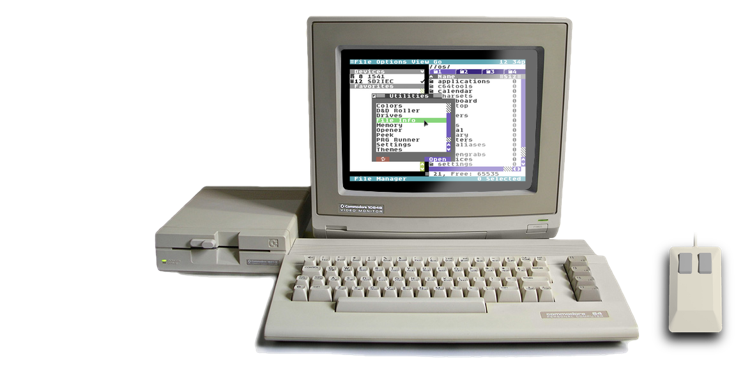
NEWS, EDITORIALS, REFERENCE
How the C64 Keyboard Works

I'm almost ashamed to admit it, but just 1 year ago when I started working on C64 OS, I didn't have the first clue how the C64 Keyboard worked. I knew there was a thing called the keyboard buffer, but I had cloudy thoughts of it being inside the keyboard itself. When I had to actually write the keyboard scanning routine for C64 and started looking at the 1982 fullspread double sided C64 schematics, I could see that the keyboard was wired up to the CIAs, but my first assumption was that when a key was pressed an IRQ would be generated. These ideas in retrospect seem embarassingly ignorant of such a basic feature of the Commodore 64.
But how are we supposed to know until we learn, right? I've written on lots of technical topics, but this post will be a deep explanation of how the C64 reads data in from the keyboard.
The CIAs (MOS 6526)
The C64 has two Complex Interface Adapter chips. Better known as the CIAs, officially the MOS 6526. You can read all about this chip on Wikipedia. But I want to explain some of my most interesting discoveries.
MOS Technology, which was acquired by Commodore and rebranded the Commodore Semiconductor Group, made a whole series of chips which I like to think of as the 65xx family. If you look up MOS 65xx on Wikipedia it'll tell you that this is a series of 8-bit microprocessors. And it's true, the 6501, 6502, 6503, 6504, 6505, 6507, 6508 and 6510, (at least) are all microprocessors. But the 65xx numbered series includes a whole family of chips that are designed to work together on a logicboard, together with some ram, rom, and other glue chips, to implement a complete microcomputer.
The C64 has a 6510 (CPU), 6567 (VIC-II, Video Interface Chip), 6581 (SID, Sound Interface Device), plus two 6526 (CIA, Complex Interface Adapter) chips. Then it has three rom chips (the shortboard reduced this to two), KERNAL, BASIC and CHARACTER roms, a bunch of RAM chips totalling to 64K, a handful of simple glue chips, in the 74xx and 74xxx series, a 556, a pair of 4066's, and most importantly the PLA (Programmable Logic Array). Together, they work beautifully to provide all that the computer is able to do.
So, what does a 6526 provide? Lots of handy things. It's got 16 registers for configuration, it's got a Time-of-Day clock with programmable alarms, it's got two 16-bit programmable timers, it's got a serial I/O port, and, most importantly for today's discussion, it has two 8-bit bi-directional ports, which we'll talk about in a minute.
What is a port, anyway?
If you'd asked me what is a port, just a year ago, I'd have said that it's a connector on the back or side of a computer, to which you can connect a peripheral device. That's half right, but it misses a couple of critical points.
A port is a line, a wire, that the CPU can control. If it's an output port that means instructions executed by the CPU can force that wire either to output +5V or GND, a logical 1 or 0 respectively. An input port means instructions executed by the CPU can read the voltage level of that line, and if it's near +5V the CPU sees this as logical 1, or near GND which the CPU reads as logical 0. There is virtually always some controlling device that allows the CPU to manage the state of that port line. And in the case of the C64 that controlling device is the 6526 CIA chip itself.
The next important thing to understand is that in a digital computer, one line (1 wire) is one bit. The wire can either be high or low, at a time. So when we say that the CIA chip has two 8-bit bi-directional ports, this no longer has to sound like gobbledygook. An 8-bit port is a port with 8 parallel, simultaenously settable or readable lines. Bi-directional means that each of those lines can be configured either as inputs or outputs. And in the case of the 6526 each line can be configured for input or output individually. At the same time some of them can be inputs and others outputs. A serial port, by the way, which the 6526 has, may as well be called a 1-bit port.
If the 6526 has two 8-bit ports, and each bit requires a line, there should be 16 lines dedicated to those ports. And indeed, when you look at the pinout diagram of the CIA above, reading down the left hand side you see PA0 through PA7, followed by PB0 through PB7. PA and PB stand for Port A and Port B, and each has 8 lines numbered 0 through 7. Amazing. That means the computer, software instructions running on the CPU, can cause those 16 chip legs to be +5V or GND, or can read the +5V or GND status of those legs.
One more step to go, the legs of the chips are connected to traces on the logicboard which run directly to a physical connector which is exposed through the chassis of the computer, and boom, it's called a port. Those physical things we've colloquially called ports our whole lives are literal technical ports, wires the CPU can independently manipulate.
How does the CPU interact with the port?
The question of course is, how does the CPU actually interact with one of those 8-bit ports? The 6526 has to be addressable, and it needs to get data from the CPU. And as we'll recall it must have one line per bit. The C64 (the 6510 CPU) has a 16-bit address bus and an 8-bit data bus, so the CIA must have 16 address legs and 8 data legs, right? Almost.
If we go back to our pinout diagram and read down the right side we see 4 legs labeled A0 through A3, and 8 labeled D0 through D7, in amongst a bunch of other lines we don't need to worry about at the moment. The Ax legs are address lines and the Dx legs are data lines. There are 8 data lines, that's good, those are obviously connected directly to the 8 data bus lines from the CPU. But why are there only 4 address lines?
As mentioned above, the 6526 has 16 configuration registers. What that actually means is that there are 16 memory addresses where the CPU can read or write to interact with the CIA. 4 bits can address from 0 to 15, and we need one line per bit, so bingo the 16 registers need only 4 address lines. But in a real C64 there are two CIAs addressed from $DC00 to $DC0F for CIA 1, and from $DD00 to $DD0F for CIA 2. Somehow, only when the upper 8 bits of the 16-bit address bus are $DC (1101 1100) or $DD (1101 1101) should CIA 1 or 2 be active respectively.
In steps the glue logic. A combination of the PLA chip (Programmable Logic Array), which is a highly custom chip created just for the C64, and a 74239 (an off the shelf 4-bit decoder), are used to monitor the upper 8-bits of the address bus and selectively turn on and off a variety of chips that are themselves connected only to the lower bits of the address bus. The 6526 is enabled or disabled via pin 23, labeled in the diagram above "/CE", for chip enable.
The fact that the chip only has 4 address lines plus a chip enable pin, rather than a full 16 address lines, means that custom glue logic can be used to map the CIA's small addressable range somewhere into a much larger address space. And, as is the case in the C64, multiple CIA chips can be mapped into different places in the main 16-bit address space.
The net result is that when the CPU sets $DC00 (1101 1100 0000 0000) onto the address bus, the PLA and 74239 together enable CIA 1, and disable every other chip on the bus. The CIA 1 chip, being enabled, sees 0000 on its 4 address lines, and the 8 data lines interact directly with whatever the 6526's register 0 actually does. We'll get to a description of the 6526's registers in a moment.
What are the CIAs hooked up to?
Now that we know what a port is, that the CIA offers two 8-bit ports, that the C64 has two CIAs, and how the C64's glue logic is setup to allow the CPU to address them, the next question is, what are those CIAs hooked up?

Above is a section of the schematics of the C64 logicboard. I've intentionally removed a number of extraneous bits around the edges to try to bring focus just on how the CIAs are wired up. In this diagram there are two main ICs shown, U1 and U2, both are labelled 6526 CIA. Their addresses are written in parentheses (DC00 - DCFF) and (DD00-DDFF)1. I added the labels in blue, #1 and #2, as they are usually referred to in documentation.
Along the left side we have four blocks. From top to bottom: Control Port 2, Control Port 1, Keyboard, and User Port. The two control ports are of course the joystick ports we all know and love on the right side of our C64. The user port is that wonderful geek port on the back of the computer at the far left. The keyboard port is a block of pins in the middle of the logic board, which the keyboard is connected to. It is as much a port as any other, but one that is only internally accessible as a result of the design of the chassis.
Let's start with the user port. You can see that pins on CIA 2 labeled PB0 through PB7, as well as PA2, run directly to pins on the user port's edge connector. Nothing could be more straight forward than that. When you plug something into the user port, you are literally connecting something directly to the Port B legs of CIA 2. Now we know why static electric discharge is so dangerous for the computer, when you touch that user port connector, you may as well be rubbing your fingers across the CIA's legs. There are no over voltage or surge protections of any kind. But at least the connection is very easy to understand.
Here's a thought. When nothing is plugged into the user port, the Port B legs of CIA 2 are very evidently not connected to anything at all. It is neither connected to a +5V source, but nor is it connected to GND. We would say that the legs are in the third state of three-state logic. That is, they're hooked up to effectively infinite resistance. In a sense they are actually connected to ground, but they are connected via a massive bridge of open air, which is highly non-conductive and thus extremely high in resistance. The question is what would the CPU read if it tried to read the values off those legs when they're hooked to nothing? The answer cannot be known by looking at the schematics alone. However, in the 6526's documentation, they are said to internally pull up. That's electronics terminology to mean, when the legs are connected to nothing, the computer will read them as logically high, or 1s rather than 0s. This is important.
How is the keyboard hooked up?
Now let's look at how the keyboard is hooked up. You can see that all 8 bits of both Port A and Port B run straight across to the keyboard connector. Port A's bits are correspondingly labeled COL0 through COL7, and Port B's bits are ROW0 to ROW7. Some of those lines branch off and up to the control ports, but we can ignore those for the moment.
The keyboard connector has just 3 additional lines, plus a spacer (KEY) to make sure you orient the cable correctly. These are +5V, GND, and a special line labeled RESTORE, which we'll get to. I took apart a C64 keyboard, shown below, so we can see what its insides look like. It was already dead, so don't worry I didn't sacrifice it in the name of science.

In the image above, I've faux-silk-screened the keycaps onto the circuit board so it's easy to see how the keys line up. Notice that the keyboard connector in the schematics labels the pins 1 through 20. On the keyboard's circuit board you can see the solder points where the wires connect, they aren't neatly in a row, but they are labeled, 0,1,2,3,4,5,6,7,8 and A,B,C,D,E,F,G,H,I. But 9 numbers and 9 letters make 18 not 20. One of those 20 is the orientation key, so it's not connected to anything, and interestingly, as we'll see, the +5V line is not needed for the keyboard, so it's not connected to anything.
Looking at the keyboard's PCB it is pretty clear that it has no electronics intelligence of any kind. It is merely a collection of switches. Each key connects two pads, and each pad is connected along a long snaking trace the joins several pads together and eventually leads to one of the 18 wires of the keyboard cable.
If we follow the traces, or better yet, use a continuity tester, we discover that the RESTORE key joins two pads which are alone on their own traces leading back to the keyboard connector. The image above doesn't show the full PCB, the function keys are missing, but you can see that from the RESTORE key's two pads the traces lead off the right side on their own. One pad is connected to the GND pin, the other to the /RESTORE pin in the schematics. Note the slash before that label, on the schematics it appears as a long bar above the word RESTORE. This means that the restore behavior is triggered by pulling the line low, or hooking it to ground. And indeed, when you press the restore key the key switch simply joins the GND line to the /RESTORE line.
Nothing else on the keyboard is connected to the /RESTORE or GND pins, the +5V pin connects to nothing, and pin 2 is just an orientation spacer, so that leaves us with 16 lines. The lines labeled COL0 through COL7 and ROW0 through ROW7, which connect to Port A and Port B of CIA 1. COL and ROW are for columns and rows, because the rest of the keys are arranged into an 8 by 8 matrix. Leaving out the RESTORE key, with its dedicated lines, if you count up all the other keys on the keyboard (and don't forget the four function keys) you get 65. Ah, but there is one other little thing to notice. The Shift Lock key is wired to exactly the same two lines as the Left Shift key. Therefore, the Shift Lock key is just a mechanically latching switch that to the computer is indistinguishable from the ordinary Left Shift key. Exclude this key, and we're left with 64 keys. And 8 times 8 is 64.
Each ROW line snakes around the board connecting to one half of the contact pads of 8 different keys. And each COL line snakes around connecting to the other half of the contact pads of 8 keys. Such that each key is a switch that connects one ROW line to one COL line. It can be a bit tricky to trace these all out visually, but a continuity tester comes in really handy. The result is that the keys are arranged in the following grid:
Commodore 64 keyboard matrix layout
| CIA 1, Port A, $DC00, write to select a column. | |||||||||
| Bit 7 $80,$7F |
Bit 6 $40,$BF |
Bit 5 $20,$DF |
Bit 4 $10,$EF |
Bit 3 $08,$F7 |
Bit 2 $04,$FB |
Bit 1 $02,$FD |
Bit 0 $01,$FE |
||
| CIA 1, Port B, $DC01, read. Each bit is a row in the selected column. |
Bit 7 $80,$7F |
Run Stop |
/ (slash) |
, (comma) |
N | V | X | Left Shift Shift Lock |
Cursor Up/Down |
| Bit 6 $40,$BF |
Q | ↑ (up arrow) |
@ (at) |
O | U | T | E | F5 | |
| Bit 5 $20,$DF |
Commodore | = (equal) |
: (colon) |
K | H | F | S | F3 | |
| Bit 4 $10,$EF |
Space | Right Shift |
. (period) |
M | B | C | Z | F1 | |
| Bit 3 $08,$F7 |
2 | Clear Home |
- (minus) |
0 | 8 | 6 | 4 | F7 | |
| Bit 2 $04,$FB |
Control | ; (semicolon) |
L | J | G | D | A | Cursor Left/Right |
|
| Bit 1 $02,$FD |
← (left arrow) |
* (asterisk) |
P | I | Y | R | W | Return | |
| Bit 0 $01,$FE |
1 | £ (pound) |
+ (plus) |
9 | 7 | 5 | 3 | Insert Delete |
|
Original Source: http://sta.c64.org/cbm64kbdlay.html. HTML reformatted, re-styled and one minor error corrected.
UPDATE: March 3, 2023
I've inverted the Rows and Columns from the way sta.c64.org had them. And it makes more sense just thinking about it. N, M, K, J, I, O, 9, 0 are physically in a column on the keyboard. They should be laid out in the table above as a column, which they now are.
Below you can see a visualization of the columns listed in the table above, superimposed over the actual C64 keyboard. The logical columns as they are wired together to the CIA chip are indeed laid out, more or less, in physical columns.
The only thing to be careful of, and these are labeled in the graphic below, is that the column selection bits of CIA 1's Port A ($DC00) are not in sequential order with the physical columns of the keyboard. I don't know why this is, but bits 1 through 6 are in order moving across the keyboard from left to right. However, the outer two columns have been swapped. Column 7 (i.e., bit 7,) is not beside Column 6; It's over on the left beside Column 1. And Column 0 is not beside Column 1; It's over on the right beside Column 6! It was at first suggested to me that this might be because of some sort of matrix layout issue. Upon further thinking about it, that cannot be the reason. To swap Column 7 and Column 0 would only require swapping those two wires coming from the CIA, this would be a trivial change. Does it date back to the PET and its weird keyboard layout? I don't know.

C64 Keyboard with the columns highlighted and their bits labeled.
We can easily spot check some of these. It is easy to see on the keyboard circuit board that W and E share a trace on the bottom half of their pads. It is also easy to spot that R and T share a trace on one half. And sure enough when we look in the table above, we can see that W and E appear in the same column. And R and T appear together in another column. Similarly, it is easy to see that Left Shift, X, V and N all share a trace. When we look in the table, sure enough, they all share a row.

I used a continuity tester to map the Letter/Number pairs of each key, which you can see in the image above. You can see several distinct patterns in keys that are physically close to each other. This also lets us map the Keyboard PCB letter/number scheme to the C64 logicboard's 20-pin keyboard connector. If we just look at PCB trace "A", we see that Space, C=, Run/Stop, and Control all share it. Looking at the key matrix table we see that this is COL 7. "B" is shared by Left Shift, Z, A, and S. Which, again from the key matrix table, we can see this is COL 1. If we look at one of the Keyboard PCB's numbered traces, say "3", it is shared by Left Shift, X, V and N. In the key matrix table these are in ROW 7. Repeating this process, we can construct the following table:
Keyboard PCB to Keyboard Connector Map
| KB PCB Label | KB Connector Pin | C64 Connection |
|---|---|---|
| A | 20 | COL7 |
| B | 19 | COL1 |
| C | 18 | COL2 |
| D | 17 | COL3 |
| E | 16 | COL4 |
| F | 15 | COL5 |
| G | 14 | COL6 |
| H | 13 | COL0 |
| I | 1 (or 3) | GND (or NMI) |
| 0 | 12 | ROW0 |
| 1 | 11 | ROW1 |
| 2 | 10 | ROW2 |
| 3 | 9 | ROW7 |
| 4 | 8 | ROW4 |
| 5 | 7 | ROW5 |
| 6 | 6 | ROW6 |
| 7 | 5 | ROW3 |
| 8 | 3 (or 1) | NMI (or GND) |
UPDATE: March 7, 2023
After updating the matrix layout table, the table before the one above, (see note on March 3, 2023,) I realized that the keyboard connector map table above had the rows and columns inverted as well. When I switched them, suddenly the pin assignment to the C64's keyboard connector jumped into an arrangement that makes perfect sense. Above you can see the table making good sense, the column and row pins are all in numeric order. Therefore, I am striking out the following paragraph, but leaving it there because these were my original musings over why the pin assignment seemed so frenetic.
I am not really sure why these numbering schemes seem so illogical. But if I had to guess it
would be a result of the physical limitations of where the traces on the logicboard have to
go such that they don't cross over each other. I'm also not sure why the letters and numbers
on the PCB don't align better with the ROW and COL numbers. For example, why is A = ROW7 and
H = ROW0? Or why is 3 = COL7 and 7 = COL3? Who knows. But if I had to guess about this, I notice
that there are extra traces connecting some of the rows and columns on the Keyboard's PCB, but
that have had holes drilled through in strategic places to sever them. This could have
been a cost saving technique for Commodore to produce the same PCB for different keyboard layouts
where the only thing they needed to do in the manufacturing process was drill some precision
holes. But I haven't (and probably won't bother) trying to figure out exactly which rows and
columns would get swapped if some different configuration of holes were present.
I can't clearly tell between "I" and "8" which goes to GND and which to NMI. Because on my keyboard the actual connector was long ago cut away. And because there is only one key, RESTORE, that joins these two together, it actually doesn't make any difference how GND and NMI are assigned to these two traces. This may all seem to be trivial information, but if you ever want to re-wire a C64 keyboard PCB (which I may someday do with the one I've got), the above table will come in handy.
How the Keyboard's PCB traces are labeled was a bit of tangent. If we return now to what is really happening, it is that when you press a key, say the H key, a wire coming off pin PA3 on CIA 1, goes into the keyboard, goes through the closed H-key switch and back out of the keyboard cable and into pin PB5 on CIA 1. Every key on the keyboard (except RESTORE) merely electrically joins one of the CIA's Port A bits to one of the CIA's Port B bits. But, how does the computer know which keys are being pressed? For that, we need to turn to the software scanning routine.
How is the keyboard matrix scanned?
When describing how the CIAs are hooked up, I mentioned something that was an important behavior. When one of the Port A or B pins is connected to nothing, it is internally pulled up such that the computer reads the value as a logical 1. When no keys are held down on the keyboard, you may have noticed that the CIA Port pins lead to the keyboard connector, and then into the keyboard, and then through traces across the keyboard's PCB but then they eventually just come to an end connecting to nothing. Therefore, no matter which CIA Port you choose to read from, as long as no keys are held down,2 those port pins are floating and they will read as 1's.
The only thing we can possibly do to change one of the port pins so that it reads as a 0 instead is to connect that pin to ground. But the only thing the pin can possibly connect to, by pressing keys and closing the circuits, is to pins on the other CIA Port. And so we are led back to the 6526 CIAs, their behaviors and how they can be configured via their registers.
Each CIA has 4 address lines, for a binary combination of 16 addressable registers. In the documentation they are referred to with their in-chip address, 0 through 15. Since we're talking about CIA #1 in the C64, and it's mapped to $DC00 to $DCFF, we use $DC00 through $DC0F to access those registers. See this article for full technical documentation of the CIA 6526.
Register's 0 and 1 are the read/write registers that correspond to Port A and Port B. However, the direction of the bits in those registers can be configured independently as either inputs or outputs. The directions of the Ports' bits are configured with registers 2 and 3 respectively. A 0 sets the corresponding bit as an input, for the CPU to read the status of something outside the computer. And a 1 sets the bit as an output, for the CPU to send data or control something outside the computer. So, to set all the bits of Port A for output, you write $11 (%11111111) to $DC02.
    LDX #%11111111
    STX $DC02 ;Port A data direction register
Since the keyboard joins the bits of Port A to the bits of Port B, and we need to pull one of those bits low, the trick is to set one of the ports as all inputs and the other as all outputs. Then we set the value of the output port as all low. This makes all of those pins a source of GND. Press a key, and the input pin is connected electrically, through the key, to a source of GND and it changes from its internally pulled-up 1 to its ground connected state, 0. When I first realized that's how it works, electrically, it was a very satisfying discovery.
    LDX #%11111111 ;Outputs
    LDY #%00000000 ;Inputs
    LDA #%00000000 ;Low/GND Outputs

    STX $DC02 ;Port A direction config
    STY $DC03 ;Port B direction config
    STA $DC00 ;Set Port A's outputs low
The problem is the following. If you press A, the low PA1 will pull PB2 low, so we know something in ROW2 was pressed. However, if you instead press D, then the low PA2 will pull PB2 low, and you would not be able to distinguish between whether it was A or D, or any other key in ROW2, that is forcing PB2 low.
In order to distinguish the columns, Port B has to be read 8 separate times. On the first loop Port A has its outputs set such that Bit 0 is low, but all the other bits are high. During that read, if a key in columns 1 through 7 (and row 2) is held down then those keys are just connecting PB2 to a high, and so they have no affect on PB2, it's already internally pulled up. However, only if the key in column 0, row 2, (Cursor Left/Right) is held down will PB2 get pulled low.
After reading Port B and storing it, we loop. Reset Port A so all the bits are high except bit 1, then read Port B again to see which keys in column 1 are down, store that, and continue until we've read 8 bytes, which are a "bitmap" of the up/down state of all 64 keys. Any set bit in the map means the corresponding key is up, any unset bit in the map is a key that is down.
And this is, more or less, what the keyboard scanning routine in the KERNAL rom does, 60 times per second. Although, it does a bunch of other stuff I'm not going to talk about today.
Concluding Thoughts
There are interesting similarities and interesting differences between how a C64 and how a PC/Mac keyboard work. PS/2, ADB and USB keyboards, even today, still use a key matrix of rows and columns that need to be scanned in order to build a table of which keys are up and which are down. However, each of these above three connection types is a serial port. In PC and Mac keyboards, the matrix scanning logic is all implemented in smart electronics inside the keyboard. The keyboard itself then maintains a memory buffer of the sequence of key codes representing up and down keys.
On a keyboard with 101 keys, assigning one code for up, and another code for down for each key, that's only 202 values, well within the 0-255 range of a single byte. The keyboard's electronics then also need to implement the serial protocol, and sends to the computer, a byte at a time, the codes representing keys going down and keys going up. It's a bit more complicated than that, and varies from serial protocol to serial protocol, but that is the essence of it.
The C64's keyboard, by comparison, is absolutely dumb (in the technical sense, not in the pejorative sense.) It has no electronics at all. Just switches in an 8x8 matrix. The actual matrix switches themselves are fed down the keyboard cable and into the computer. And the C64's own CPU needs to spend precious time scanning the matrix. It is truly unfortunate that on a machine with only 1MHz to spare, it needs to use some non-trivial number of those cycles, because whatever it takes to fully scan the matrix once, has to be repeated 60 times a second, just to input data from the keyboard.
But on PCs with thousands of times the number of cycles available, it doesn't need to spend any of those cycles worrying about scanning the keyboard. If the state of the keyboard isn't changing, the internal logic of the keyboard is figuring that out, and it doesn't have to send any data to the computer via its serial connection. And there you have it.
Feel free to leave, questions, comments and corrections in the comments!
-
The careful observer may notice that on the schematic the address range is DC00 to DCFF,
instead of DC00 to DC0F. The PLA and 74239 map in the CIAs whenever the upper 8 bits
are $DC (or $DD), even though the CIAs are only connected to the lowest 4 bits of the
address bus.
When a CIA is mapped in, bits 4 to 7 are completely ignored. The effect of this is that the CIAs appear to be mirrored 16 times across DCx0 to DCxF. It is not recommended to address them above DC0x (or DD0x) because future Commodore models could include additional glue logic for mapping other components into those higher address ranges. And, in fact, I believe the C128 does this very thing for accessing its extended keyboard. [↩] - Also assuming none of the joystick/control port lines are connected to anything, but I'm leaving aside the control ports in this post to focus on the keyboard. [↩]
Do you like what you see?
You've just read one of my high-quality, long-form, weblog posts, for free! First, thank you for your interest, it makes producing this content feel worthwhile. I love to hear your input and feedback in the forums below. And I do my best to answer every question.
I'm creating C64 OS and documenting my progress along the way, to give something to you and contribute to the Commodore community. Please consider purchasing one of the items I am currently offering or making a small donation, to help me continue to bring you updates, in-depth technical discussions and programming reference. Your generous support is greatly appreciated.
Greg Naçu — C64OS.com